“Materials are like people: It is the defects in them that tend to make them interesting,” Arizona State University scientist Sefaattin Tongay says in explaining the root of his research, paraphrasing renowned British materials scientist and physicist Sir Colin Humphrey.
Tongay’s focus is on 2-D materials — one of the thinnest of all materials, only 0.7 nanometer thick — and the myriad functions they can perform when their crystalline atomic structures are less than perfect.
His overarching goal is to discover how to create the precise kinds of imperfections in 2-D materials to maximize their potential in energy conversion and information technologies.
Sometimes called single-layer materials, each of these crystalline layers measures only a few atoms in thickness. Researchers have discovered that defects in them are not necessarily problems, but opportunities.
Due to their extreme thinness, the electrical and optical properties of 2-D materials can be qualitatively and quantitatively different than those of the 3-D materials that have been conventionally used in semiconductor technology.
Those differences often mean they can exceed the efficiency of other materials at absorbing and emitting light, transmitting an electrical charge or conducting heat.
Applications in many technologies
The combination of the unusual properties of 2-D materials can “lead to a wide range of novel devices and other technology with defense, aerospace, medical, energy and industrial applications,” said Tongay, an assistant professor of materials science and engineering in ASU’s Ira A. Fulton Schools of Engineering.
The materials’ distinctive properties could lead to applications that improve lighting technologies such as light-emitting diodes (LEDs), as well as batteries, cellphones, flexible electronics, biosensors and the photovoltaic cells used to convert sunlight into energy.
Tongay’s work recently earned him National Science Foundation (NSF) CAREER Award, which is given to scientists and engineers who are demonstrating potential to become national leaders in research and education in their areas of expertise.
The award will provide him $501,000 over five years to pursue new discoveries and applications of 2-D materials, as well as provide opportunities for students and the public to learn more about the field and what it promises to contribute to society.
Creating defects to engineer useful functions
Tongay’s research team will seek to further reveal the fundamental physics of defects in 2-D materials, in particular those with semiconducting capabilities.
The goal is to measure, analyze and establish the roles of the structural defects in shaping the optical and electronic properties of select 2-D semiconducting materials and to explore new ways to control their specific properties.
It’s missing or foreign atoms in a material that cause such defects, which break the periodicity in a material’s otherwise uniform atomic configuration.
“We are looking at ways to introduce certain kinds of defects into the materials and manipulating them to perform useful functions,” Tongay said. “We want to engineer these properties so that we can realize the full potential of 2D materials.”
Deep exploration into how materials behave
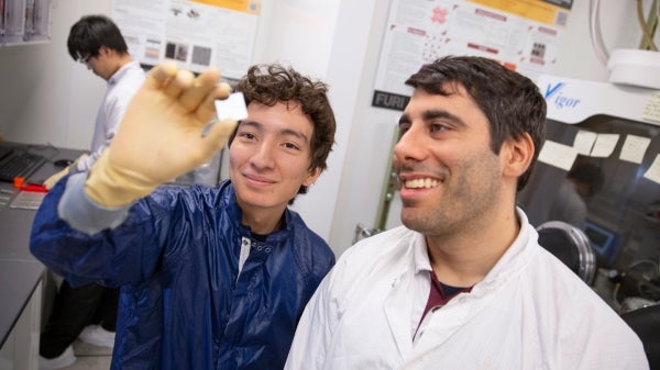
Using ASU’s advanced transmission electron microscopy facilities, “you can tell how the atoms are configured in the materials. You can look as you use lasers to knock atoms out of the material or bombard it with ions to engineer imperfections, and you can tell how the structures look different before and after the impact,” he said.
This technique will enable Tongay’s lab team to see how defects progress, how they change in real time, how they rearrange themselves and recombine.
“We can look at how the materials behave in these situations in spans of only microseconds, which is really impressive,” he said.
From there, the researchers intend to learn how specific patterns of defects can yield materials capable of functions that could produce myriad advances in electronics, and solutions to some of the world’s major technological challenges.
Spreading awareness of 2-D materials
Findings from the project will be made available to other engineers, scientists and the public through 2DLibrary.org, a website that Tongay’s group will build to provide an open-access database focused on 2-D materials and the study of their defects. The nonprofit organization that owns the website Materialsproject.org and two mainstream 2-D materials companies will collaborate on developing the database.
The NSF award will also support Tongay’s education outreach efforts.
He’ll initiate a program called NanoSciED (for Nanoscience Education) to bring knowledge of his field to the public through ASU outreach events such as Discover-E Day and Night of the Open Door.
NanoSciED will organize and host summer camps for high school students, including those from underserved communities, to introduce them to the world of materials — with the aim of instilling in them an interest in STEM (science, technology, engineering and math) fields.
Undergraduate students will have an opportunity to participate in lab work under Tongay’s mentorship through ASU’s Fulton Undergraduate Research Initiative (FURI). In addition, a number of graduate students pursuing their master’s or doctoral degrees will have key roles on the research team.
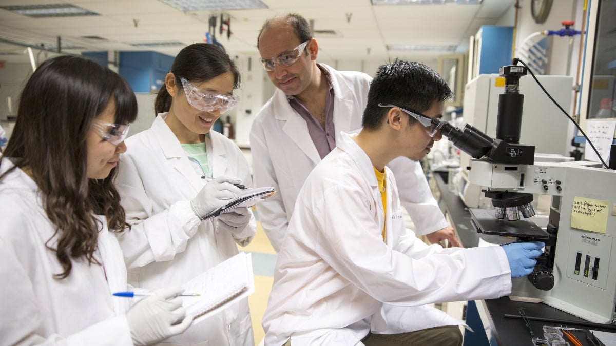
Top photo: Assistant professor of materials science and engineering Sefaattin Tongay (second from right) has earned a CAREER Award from the National Science Foundation to support his research on the use of 2-D materials to develop advances in a variety of technologies. The project provides opportunities for laboratory experience for graduate students and postgraduates. Pictured with Tongay are (from left) master’s student Xi Fan, postdoctoral researcher Xiuqing Meng and master’s student Wilson Kong. They are inspecting synthesized 2-D materials and discussing their findings. Photo by Jessica Hochreiter/ASU
More Science and technology

ASU researcher part of team discovering ways to fight drug-resistant bacteria
A new study published in the Science Advances journal featuring Arizona State University researchers has found vulnerabilities in certain strains of bacteria that are antibiotic resistant, just…

ASU student researchers get early, hands-on experience in engineering research
Using computer science to aid endangered species reintroduction, enhance software engineering education and improve semiconductor material performance are just some of the ways Arizona State…

ASU professor honored with prestigious award for being a cybersecurity trailblazer
At first, he thought it was a drill.On Sept. 11, 2001, Gail-Joon Ahn sat in a conference room in Fort Meade, Maryland. The cybersecurity researcher was part of a group that had been invited…
