5 microelectronics projects win nearly $30M in federal funding

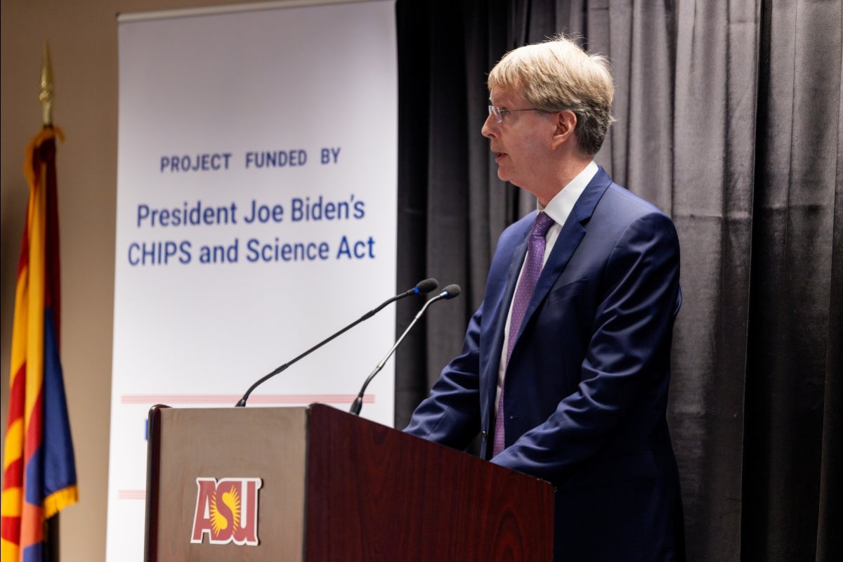
Tarun Chhabra, deputy assistant to the president and coordinator for technology and national security, said the projects will reduce the gap between laboratory prototyping and fabrication. Photo by Samantha Chow/ASU News
The five projects will help strengthen the nation's chip-making capabilities and reduce dependency on foreign sources of microelectronics. They are among 33 projects across the nation awarded a total of $269 million under the bipartisan CHIPS and Science Act-funded Microelectronics Commons initiative, as announced by the U.S. Department of Defense on Tuesday.
White House and U.S. Department of Defense officials began a three-city nationwide tour to announce these projects with a visit to the ASU MacroTechnology Works on Tuesday to reveal details of the projects in Arizona, as well as those from two hubs in California.
ASU has been instrumental in the development of the Southwest Advanced Prototyping Hub, or SWAP Hub, serving as a convener and a leader in promoting innovation and collaboration, according to Sally C. Morton, executive vice president of ASU Knowledge Enterprise.
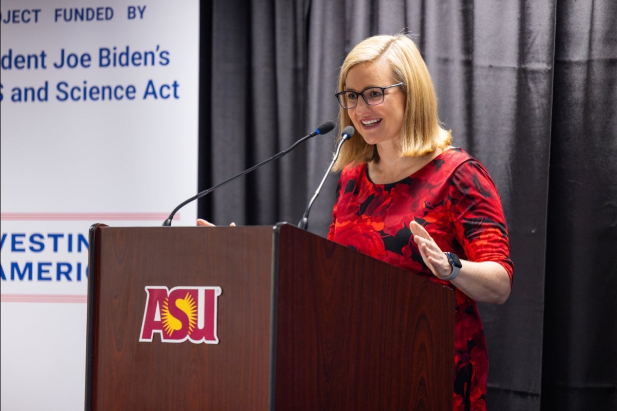
“SWAP Hub, along with our partners, leverages the collective expertise of our dedicated faculty and students at Arizona State University’s Fulton Schools to ensure a vital, sustainable and prosperous future for the region,” she said.
“By bringing together researchers and industry leaders, we have helped drive advancements in technology that are transforming industries and boosting economic growth.”
Headquartered in Arizona, the SWAP Hub is part of the Microelectronics Commons, a nationwide network of eight regional technology hubs. It connects the Southwest — the fastest-growing and largest semiconductor cluster in the U.S., with more than $100 billion in private investment — to a growing network of defense and electronics partners across the country.
The Microelectronic Commons, established in 2023, is set to receive a total of $2 billion through 2027. The initiative focuses on bridging the gap between laboratory prototyping and fabrication, according to Tarun Chhabra, deputy assistant to the president and coordinator for technology and national security, who spoke at Tuesday’s event.
“Well, $2 billion is, of course, a lot of money in absolute terms, but between the local and national levels, China is pumping hundreds of billion dollars into their chip manufacturing design equipment and materials investments,” Chhabra said.
“And their goal is not just self-reliance, but to dominate the global chip industry. And we can't let that happen.
“So we will not match China dollar for dollar, but we can outcompete them with the talent and with the resources that we are investing today in kicking off these Hub programs.”
Workforce development is a critical component of the initiative. Kyle Squires, dean of the Ira A. Fulton Schools of Engineering at ASU and CEO of the SWAP Hub, told the group that ASU has enrolled almost 33,000 engineering students this fall.
“Many of these talented young men and women will be the workforce of tomorrow,” he said.
“They'll leverage the investments we're talking about today — and the work in discovery that will emerge from it — into this future that we're hearing about, where we lead the world not only in research discovery and innovation, but also in manufacturing.”
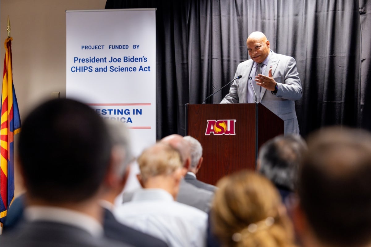
In the first year, the Microelectronics Commons have already produced results, according to Maynard Holliday, who was at the event to perform the duties of assistant secretary of defense for critical technologies in the Office of the Under Secretary of Defense for Research and Engineering.
He cited the partnership between ASU and DECA Technologies to collaborate on North America’s first Fan-Out Wafer-Level Packaging (FOWLP) research and development capability.
“This center will combine state-of-the-art advanced-packaging technology, equipment, processes, materials, expertise and training, fostering the development of new capabilities from proof of concept to pilot scale,” he said.
The five SWAP Hub projects that were awarded $29.6 million this week are:
Integrated RF GaN Technology to Support NextG, 5G & 6G Wireless Systems: The project team is NXP, Raytheon, National Instruments and ASU. As data consumption skyrockets, telecommunications systems must operate at higher frequencies and wider bandwidths while meeting stringent size, weight and power requirements. The project aims to integrate advanced reconfigurable radio architectures with gallium nitride technology to create a unified, self-testing system.
SMART — Scalable Modular Architecture for RF Transceivers: The project team is Alphacore, ASU, Rice University, Lockheed Martin and Auburn University. The project aims to advance radio frequency transceiver technology to improve national defense and commercial capabilities. Integrating communications and sensing in a single system-on-a-chip increases resource efficiency, optimizes spectrum utilization, reduces latency and improves reliability while reducing the size and cost of transceivers. The goal of the project is to create a transceiver integrated on a single microelectronics chip, capable of both communications and sensing functions with novel capabilities for devices using 5G and 6G mobile networks and beyond
Spaceborne Low-Energy AI Computing: The project team is ASU, Sandia National Laboratories, Raytheon, the University of Southern California, the University of Colorado at Boulder, LTC Design, Air Force Research Laboratory and Global Foundries. Advancing the performance of satellites through artificial intelligence could yield a major advantage for national defense. This project aims to extend the power of AI to satellites orbiting the planet by directly integrating a highly efficient, radiation-hard AI chip with focal plane array image sensors used in space. This would be several times more efficient than modern unhardened systems and over 100 times more efficient than the current radiation-hard systems and will enable satellites to track objects that are too faint or too fast to be detected by current systems.
Multi-MHz, High Density, Ultra-fast RADAR Power Converter: The project team is ASU, Sandia, Infineon, Lockheed Martin and ThermAvant. This project will advance radar power systems in critical defense applications by developing a multi-megahertz, multi-kilowatt, high-density ultra-fast radar power converter that forms the heart of advanced radar systems. The converters will use gallium nitride-based switching devices that dramatically improve performance — including six times higher power density, 50% lower losses and ultra-fast response times.
ARC-V Secure Processor: The project team is Idaho Scientific, Synopsys, Global Foundries, Mercury Computer and BAE Systems. The project’s primary objective is to create a secure, low-power processor that allows the military to confidently deploy advanced systems, even in contested environments, that rely on powerful but vulnerable commercial electronics. The secondary objective is to develop a customer reference design and software development kit that allows both commercial and military users to evaluate the performance and security features of the ARC-V Secure Processor.
“The SWAP Hub has developed an unmatched network of partner capabilities that reflect the objectives and intentions of the Microelectronics Commons, and these project awards enable us to translate the Hub’s capabilities into impact by solving pressing national security technology challenges.”
The SWAP Hub has more than 170 members — 75 large companies, 28 academic institutions and more than 60 small businesses. One of those is Sandia National Laboratories, which has been one of America’s leading research and development labs working on national security-related projects since 1949.
“The SWAP Hub's focus on extreme environments and hardware assurance/security aligns strategically with Sandia’s missions, fostering the growth of future microelectronics innovation and leadership in this critical national security sector," said Reno Sanchez, director of the Microsystems Engineering, Science and Applications Center at Sandia.
“Sandia is proud to support the vital work of the SWAP Hub. This partnership will enhance the U.S. pipeline for high-reliability, secure semiconductors and create workforce development opportunities.”
During their visit, officials also announced that the California Defense Ready Electronics and Microdevices Superhub, led by the University of Southern California's Information Sciences Institute, and the California Pacific-Northwest AI Hardware Hub, led by Stanford University, also received funding for projects under the Microelectronics Commons initiatives.
More Science and technology

ASU-led space telescope is ready to fly
The Star Planet Activity Research CubeSat, or SPARCS, a small space telescope that will monitor the flares and sunspot activity of low-mass stars, has now passed its pre-shipment review by NASA.…

ASU at the heart of the state's revitalized microelectronics industry
A stronger local economy, more reliable technology, and a future where our computers and devices do the impossible: that’s the transformation ASU is driving through its microelectronics research…

Breakthrough copper alloy achieves unprecedented high-temperature performance
A team of researchers from Arizona State University, the U.S. Army Research Laboratory, Lehigh University and Louisiana State University has developed a groundbreaking high-temperature copper alloy…


