From Belarus to Intel: Going the distance to advance semiconductor manufacturing

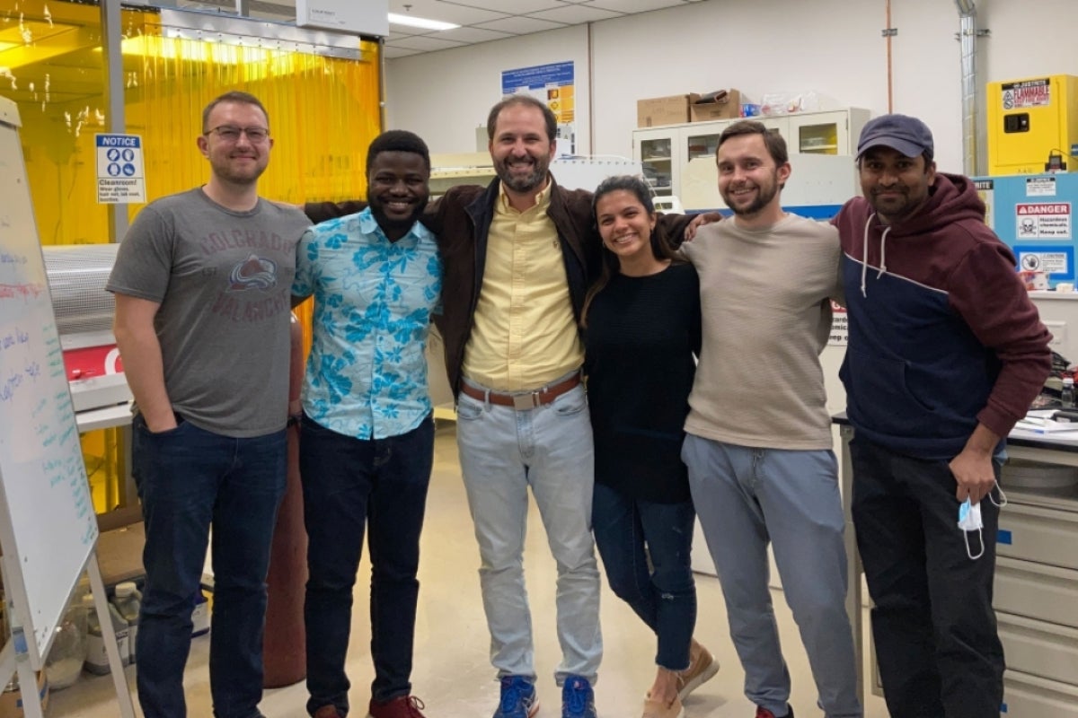
Bruno Azeredo (second from left), an assistant professor of manufacturing engineering in the Ira A. Fulton Schools of Engineering at Arizona State University, has three doctoral students who are starting jobs at Intel: Amm Hasib (far left), Aliaksandr "Sasha" Sharstniou (second from right) and Stanislau "Stas" Niauzorau (far right). Photo courtesy Bruno Azeredo
When Aliaksandr “Sasha” Sharstniou was starting as an undergraduate student in Belarus, he didn’t know where life would take him. He just knew he liked physics, chemistry and making things with his own hands — all interests he’d learn would serve him well in semiconductor manufacturing.
During one of his undergraduate semiconductor laboratory classes in Belarus, Sharstniou was getting bored with an extensive lesson on old bipolar transistors. He knew it was important background knowledge, but he spoke up about wanting to move on and talk about newer and more advanced semiconductor transistor technologies.
In response, his lab instructor said, “It’s not like you’re going to be working at Intel,” before continuing with the lesson.
Sharstniou didn’t think much of that statement at the time. He was eager to learn about semiconductors, but he didn’t expect to one day move to the United States and get a job at a top company like Intel working on the latest semiconductor research. However, 10 years later, that’s exactly where he is.
“I never thought I would have this opportunity,” Sharstniou says. “You never know where you will end up.”
Sharstinou is now preparing to begin a new position as a packaging R&D engineer at the Intel advanced packaging research and development facilities in Arizona after earning his doctorate in materials science and engineering from the Ira A. Fulton Schools of Engineering at Arizona State University.
His doctoral research has focused on creating a scalable fabrication process for optoelectronic semiconductor devices called metal-assisted electrochemical nanoimprinting, or Mac-Imprint. Sharstniou’s innovative technique, for which he holds a U.S. patent, could contribute to industrial advances in semiconductor manufacturing processes used in Arizona and beyond over the next five or 10 years.
Bruno Azeredo, an assistant professor of manufacturing engineering who has been Sharstniou’s advisor for the past five and a half years, says his work is helping to overcome a major hurdle in the semiconductor industry’s quest to develop microelectronics that use optics, or signals made of light, instead of electrical signals.
“Miniaturizing fiber optics has been a gigantic challenge both from a design standpoint because the devices have to be designed in novel ways, and in manufacturing, because it involves heterogeneous materials and novel manufacturing processes,” says Azeredo, a faculty member in the School of Manufacturing Systems and Networks, part of the Fulton Schools. “Sasha’s contribution is developing a way to make these optical materials with silicon and delivering metrics in resolution, 3D structuring and scalability that are so relevant.”
Though he has put in a lot of hard work to get to this point, Sharstniou says much of his success has come down to luck.
“I’m just a lucky person to meet and be surrounded by good people under the right circumstances,” he says.
Overcoming hardships to start his journey
Raised by a single mother and his grandparents in Vitebsk, Belarus, Sharstniou and his family struggled financially.
“My mom is a doctor, but in Belarus, doctors are not paid very well, so she had to work several shifts to make a living,” Sharstniou says. “Now I realize how much she was doing to make things work and I was lucky to have what I had back then.”
Sharstniou was fortunate his family was still able to find ways to foster his interests. He had books to learn about physics and chemistry, and later, his mother could afford to buy a computer and dial-up internet. Sharstniou attended a good high school and studied hard to pass his exams.
“I know that a lot of kids in Belarus back in the day didn’t have these opportunities,” he says. “They might have the brains for it, but not the opportunity to get there.”
After high school, his family helped him attend the Belarusian State University of Informatics and Radioelectronics, where he received a strong educational foundation that would support his future pursuits.
There, he met Associate Professor Vitaly Bondarenko in an undergraduate microelectronics class. Bondarenko led the Nanoelectronic Materials and Structures Laboratory, where his research group studied electrochemical methods of semiconductor processing and other topics.
“I liked him as a person and I liked his course,” Sharstniou says about Bondarenko. “I asked if I could join his research group as an undergraduate researcher and he was kind enough to allow me to do it.”
There, he conducted research on the fabrication of porous silicon and deposition of zinc oxide nanostructures onto it.
Research not only taught him technical skills, but Sharstniou says it also “definitely taught me about critical thinking, the careful design of experiments and about thoroughness.”
A serendipitous start to a doctoral degree
With his friend and classmate Stanislau “Stas” Niauzorau, Sharstniou was lucky again to meet an important person who would lead him to the next stage of his education and research pursuits.
While attending a semiconductor conference in Spain, Sharstniou and Niauzorau met Azeredo, who was just about to start a new faculty position at ASU.
Sharstniou personally got along well with Azeredo, and says, “I think he really liked my background, my expertise, and that’s how I got the offer to join his group.”
Azeredo remembers meeting two young researchers with an excellent electrochemistry foundation who were interested in and knowledgeable about his work. He also recalls them both jumping into the cold, winter ocean after a conference event.
Inviting these smart and intriguing researchers to join his lab was also an important moment for Azeredo. As a new assistant professor at ASU, he was preparing to walk into an empty room and start his lab from scratch.
“Your first PhD students are the people who build everything you see in the lab,” Azeredo says. “Together, we developed a unique way to micromachine silicon, and I think they really helped me realize the vision that electrochemistry can be used to micromachine silicon.”
Sharstniou was excited about this opportunity, but getting to ASU to join the lab was difficult. He couldn’t even afford the plane ticket to the U.S., and he had to leave behind his wife, Aksana Atrashkevich, who was still finishing her bachelor’s degree in Belarus. But again, his family came together to help support his dreams, raising enough money to help him move. Sharstniou was glad to have his friend Niauzorau — who has become like a brother — with him.
“I liked how Stas and I worked on building Bruno’s lab from scratch because I never had this experience before,” Sharstniou says. “Being able to participate in the discussions of what we need, what is the future direction of the lab and how it will be developed — it was a very unique experience that I will cherish. It led to several months of overnight work, but I also liked it because I was working with my friend.”
Achieving success at ASU
One of Sharstniou’s most memorable achievements at ASU was when he finally got to hold something he made — a successful result of his innovative fabrication technique — in his own hands.
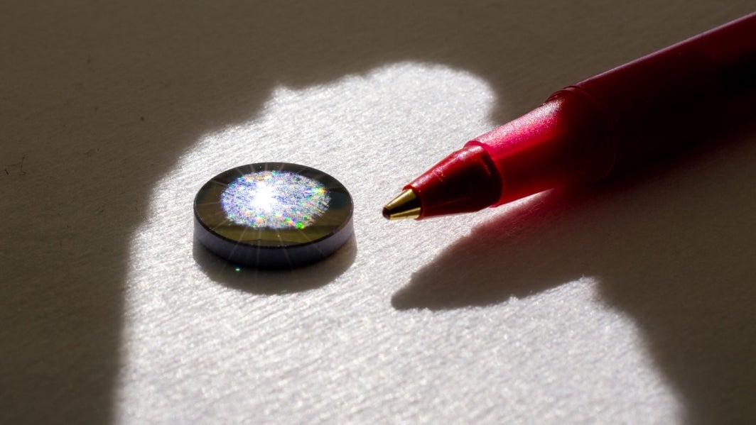
Optical metasurfaces require the creation of tiny 3D structures that interact with light in a unique way. Sharstniou was tasked with fabricating those structures on a silicon lens to demonstrate the versatility of the Mac-Imprint process. The technique involves pressing a 3D stamp coated in a noble metal like gold against a silicon lens while immersed in a chemical solution. Using an electrochemical corrosion process, 3D features of the stamp are then etched, or “imprinted,” onto the lens.
“It was kind of a crazy idea. We took flexible, stretchable nanosponges that are typically meant to filter water and inflated them like a balloon to conform to the surface of the lens,” Azeredo says. “As a graduate student, I didn’t think of doing some of the things he did, so I’m proud of him.”
Azeredo and Sharstniou remember the first time the process was successful after years of work. Seeing the etched surface of the silicon lens diffract a rainbow of colors was a huge moment of joy.
Earlier parts of this work provided a significant amount of the preliminary results that led to Azeredo earning a prestigious 2020 National Science Foundation Faculty Early Career Development Program (CAREER) Award.
Sharstniou’s major contributions to this research over the past few years also contributed to him being the first author of research papers published in the Proceedings of the National Academy of Sciences and Advanced Materials, two of the top journals for science and engineering.
With the help of Azeredo, his other collaborators and the resources at ASU — lab facilities including the Eyring Materials Center and access to the latest research literature, things he only dreamed about in Belarus — Sharstniou has had an amazing journey, and it’s still in progress.
A bright future awaits
Azeredo says Sharstniou had many colleagues at top-10 universities interested in bringing him to their teams as a postdoctoral researcher. His skills in a variety of fields — electrochemistry, electrical and mechanical engineering, materials science and more — are in high demand.
However, meeting his new manager at Intel made Sharstniou sure about his choice to join Intel and start his industry career.
“I liked how he approached the interview process. I liked his attitude and how open and willing to help he was,” Sharstniou says. “I think that personal relationships in work are important — that’s why I work so well with Bruno and my friend Stas — and I think that’s what will happen at Intel.”
He anticipates his job will involve building a state-of-the-art lab and developing new technologies, processes and equipment for semiconductor chip interconnects in a highly research-oriented position.
In addition to the exciting prospects of this new career, this accomplishment means a lot to Sharstniou and his family in other ways.
His wife joined him in the U.S. in 2018 and was accepted into the environmental engineering doctoral program under Fulton Schools Assistant Professor Sergi Garcia-Segura. Sharstniou says his wife has been a major inspiration.
“When she came here, she wasn't thinking about joining a PhD program, but she worked her way to be admitted to a program she didn't have any experience with from Belarus,” he says. “She has this inner strength and can work through anything. It’s very impressive.”
Now that he’s not always occupied with the all-consuming work of a doctoral student, he can dedicate more time to his wife and family, and give back to his mother, who was the foundation of this achievement.
Sharstniou still doesn’t know where life will take him now that he’s starting his career at Intel. For now, he is looking forward to conducting research that could soon be applied to improve manufacturing processes — and people’s lives.
“Understanding that your efforts are actually used to make people’s lives better, that is important to me,” he says. “I hope my future work will do that.”
Help enable Ira A. Fulton Schools of Engineering students to overcome financial obstacles and be successful by donating to the Fulton Schools of Engineering International Student Support Fund and the Fulton Student Emergency Fund.
More Science and technology

ASU-led space telescope is ready to fly
The Star Planet Activity Research CubeSat, or SPARCS, a small space telescope that will monitor the flares and sunspot activity…

ASU at the heart of the state's revitalized microelectronics industry
A stronger local economy, more reliable technology, and a future where our computers and devices do the impossible: that’s the…

Breakthrough copper alloy achieves unprecedented high-temperature performance
A team of researchers from Arizona State University, the U.S. Army Research Laboratory, Lehigh University and Louisiana State…


